- 您现在的位置:买卖IC网 > Sheet目录333 > IRS26072DSPBF (International Rectifier)IC DVR HI/LOW SIDE 600V 8-SOIC
�� �
�
�IRS26072DSPbF�
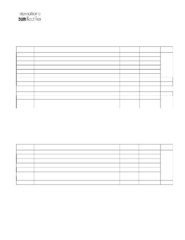
�Absolute� Maximum� Ratings�
�Absolute� maximum� ratings� indicate� sustained� limits� beyond� which� damage� to� the� device� may� occur.� All� voltage�
�parameters� are� absolute� voltages� referenced� to� COM� unless� otherwise� specified.� The� thermal� resistance� and�
�power� dissipation� ratings� are� measured� under� board� mounted� and� still� air� conditions.�
�V� B� -� 20�
�20�
�Symbol�
�V� B�
�V� S�
�V� HO�
�V� CC�
�V� LO�
�V� IN�
�PW� HIN�
�dV� S� /dt�
�P� D�
�Rth� JA�
�T� J�
�T� S�
�T� L�
�Definition�
�High� side� floating� supply� voltage�
�High� side� floating� supply� offset� voltage�
�High� side� floating� output� voltage�
�Low� side� and� logic� fixed� supply� voltage�
�Low� side� output� voltage�
�Logic� and� analog� input� voltages�
�High-side� input� pulse� width�
�Allowable� offset� supply� voltage� slew� rate�
�Package� power� dissipation� @� TA� ≤� +25°C�
�Thermal� resistance,� junction� to� ambient�
�Junction� temperature�
�Storage� temperature�
�Lead� temperature� (soldering,� 10� seconds)�
�Min.�
�-0.3�
�?�
�V� S� -� 0.3�
�-0.3�
�-0.3�
�-0.3�
�500�
�—�
�—�
�—�
�—�
�-50�
�—�
�Max.�
�620�
�V� B� +� 0.3�
�V� B� +� 0.3�
�?�
�V� CC� +� 0.3�
�V� CC� +� 0.3�
�—�
�50�
�0.625�
�200�
�150�
�150�
�300�
�Units�
�V�
�ns�
�V/ns�
�W�
�°C/W�
�°C�
�?�
�All� supplies� are� fully� tested� at� 25� V.� An� internal� 20� V� clamp� exists� for� each� supply.�
�Recommended� Operating� Conditions�
�For� proper� operation,� the� device� should� be� used� within� the� recommended� conditions.� All� voltage� parameters� are�
�absolute� voltages� referenced� to� COM� unless� otherwise� specified.� The� V� S� offset� ratings� are� tested� with� all� supplies�
�biased� at� 15� V.�
�Symbol�
�V� B�
�Definition�
�High� side� floating� supply� voltage�
�Min.�
�V� S� +10�
�Max.�
�V� S� +� 20�
�Units�
�V� S�
�Static� high� side� floating� supply� offset� voltage�
�?�
�-8�
�600�
�Transient� high� side� floating� supply� offset� voltage�
�V� S� (t)�
�??�
�-50�
�600�
�V� HO�
�V� CC�
�V� LO�
�V� IN�
�T� A�
�High� side� floating� output� voltage�
�Low� side� and� logic� fixed� supply� voltage�
�Low� side� output� voltage�
�Logic� input� voltage�
�Ambient� temperature�
�V� S�
�10�
�0�
�0�
�-40�
�V� B�
�20�
�V� CC�
�V� CC�
�125�
�V�
�°C�
�?�
�??�
�Logic� operation� for� V� S� of� –8� V� to� 600� V.� Logic� state� held� for� V� S� of� –8� V� to� –V� BS� .�
�Operational� for� transient� negative� V� S� of� -50� V� with� a� 50� ns� pulse� width.� Guaranteed� by� design.� Refer� to� the�
�Application� Information� section� of� this� datasheet� for� more� details.�
�www.irf.com�
�6�
�?� 2009� International� Rectifier�
�发布紧急采购,3分钟左右您将得到回复。
相关PDF资料
IRS2607DSTRPBF
IC DVR MOSFET/IGBT N-CH 8-SOIC
IRS2608DSTRPBF
IC DRIVER MOSFET/IGBT 8-SOIC
IRS2609DSPBF
IC DVR MOSFET/IGBT N-CH 8-SOIC
IRS26302DJTRPBF
IC GATE DRIVER 3PH BRIDGE 44PLCC
IRS26310DJTRPBF
IC DRIVER MOSFET/IGBT 44-PLCC
IRS4427PBF
IC MOSFET DRIVER
IRS4427SPBF
IC DVR LOW SIDE DUAL 8-SOIC
IRS4428STRPBF
IC DVR LOW SIDE DUAL 8-SOIC
相关代理商/技术参数
IRS26072DSPBF_11
制造商:IRF 制造商全称:International Rectifier 功能描述:HIGH AND LOW SIDE DRIVER
IRS26072DSTRPBF
功能描述:功率驱动器IC Hlf-Brdg Drvr IC motion Cntrl IC
RoHS:否 制造商:Micrel 产品:MOSFET Gate Drivers 类型:Low Cost High or Low Side MOSFET Driver 上升时间: 下降时间: 电源电压-最大:30 V 电源电压-最小:2.75 V 电源电流: 最大功率耗散: 最大工作温度:+ 85 C 安装风格:SMD/SMT 封装 / 箱体:SOIC-8 封装:Tube
IRS2607DSPBF
功能描述:功率驱动器IC 600V High Low 10 to 20V 530ns RoHS:否 制造商:Micrel 产品:MOSFET Gate Drivers 类型:Low Cost High or Low Side MOSFET Driver 上升时间: 下降时间: 电源电压-最大:30 V 电源电压-最小:2.75 V 电源电流: 最大功率耗散: 最大工作温度:+ 85 C 安装风格:SMD/SMT 封装 / 箱体:SOIC-8 封装:Tube
IRS2607DSPBF
制造商:International Rectifier 功能描述:DRIVER
IRS2607DSTRPBF
功能描述:功率驱动器IC Half Bridge Drvr Hi Volt & Hi Speed
RoHS:否 制造商:Micrel 产品:MOSFET Gate Drivers 类型:Low Cost High or Low Side MOSFET Driver 上升时间: 下降时间: 电源电压-最大:30 V 电源电压-最小:2.75 V 电源电流: 最大功率耗散: 最大工作温度:+ 85 C 安装风格:SMD/SMT 封装 / 箱体:SOIC-8 封装:Tube
IRS2608DSPBF
功能描述:功率驱动器IC 600V Half-Bridge 10 to 20V 530ns RoHS:否 制造商:Micrel 产品:MOSFET Gate Drivers 类型:Low Cost High or Low Side MOSFET Driver 上升时间: 下降时间: 电源电压-最大:30 V 电源电压-最小:2.75 V 电源电流: 最大功率耗散: 最大工作温度:+ 85 C 安装风格:SMD/SMT 封装 / 箱体:SOIC-8 封装:Tube
IRS2608DSPBF_1
制造商:IRF 制造商全称:International Rectifier 功能描述:HALF-BRIDGE DRIVER
IRS2608DSTRPBF
功能描述:功率驱动器IC Hlf Brdg Drvr 600V .250A Compl Inpt
RoHS:否 制造商:Micrel 产品:MOSFET Gate Drivers 类型:Low Cost High or Low Side MOSFET Driver 上升时间: 下降时间: 电源电压-最大:30 V 电源电压-最小:2.75 V 电源电流: 最大功率耗散: 最大工作温度:+ 85 C 安装风格:SMD/SMT 封装 / 箱体:SOIC-8 封装:Tube